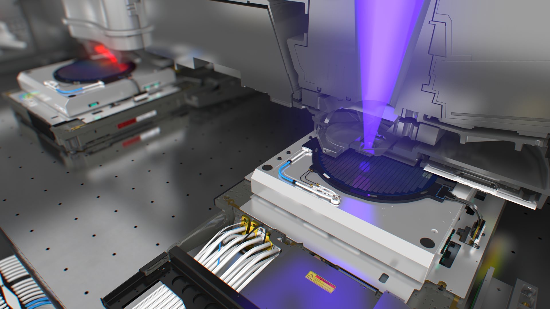
Dutch semiconductor equipment giant ASML has quietly achieved what could be a game-changer for global chip production: a stable, high-power extreme ultraviolet (EUV) light source capable of sustaining 1,000 watts—nearly double the current 600W standard. The innovation isn’t just incremental; it promises to boost wafer output by up to 50% over the next decade without requiring fabs to expand their physical footprint or deploy entirely new machines.
For an industry still grappling with AI-driven demand surges and supply chain fragility, the timing couldn’t be better. TSMC, Samsung, and Intel have all scrambled to ramp up capacity, but ASML’s solution—if widely adopted—could alleviate some of the pressure without the years-long lead time of building additional fabs.
From 220 to 330 Wafers per Hour
The core of the breakthrough lies in ASML’s ability to sustain a 1,000W EUV light source under the same operational constraints as today’s systems. While competitors have demonstrated fleeting bursts of higher power in lab settings, ASML claims its new system delivers consistent performance—critical for mass production. The result? A projected jump from 220 wafers per hour to 330, all while maintaining cost efficiency.
This isn’t just about brute-force power, though. ASML’s approach leverages Productivity Enhancement Packages (PEPs), modular upgrades that can be retrofitted to existing machines—including older NXE:3400C/D models—without requiring a full system overhaul. For newer NXE:3800E setups and the upcoming High-NA EXE:5000/5200 series, the upgrade path appears even smoother.
Challenges Ahead: Power, Cooling, and Adoption
Yet scaling this innovation won’t be without hurdles. Higher power demands translate to significant changes in cooling systems and hydrogen gas flow—both of which must be carefully managed to avoid equipment degradation. ASML’s Michael Purvis emphasized that this isn’t a laboratory stunt; it’s a production-ready system tested under real-world conditions. Still, fabs will need to assess whether their infrastructure can handle the transition.
Another question looms over adoption: Will chipmakers prioritize upgrading existing EUV tools over investing in next-generation High-NA systems? The latter, capable of printing even finer features at 2nm and beyond, remains a long-term bet. For now, ASML’s kilowatt EUV could serve as a bridge, offering immediate relief to an industry desperate for capacity.
A Silver Bullet for AI’s Hungry Appetite?
The stakes are higher than ever. AI data centers—already consuming vast quantities of GPUs and TPUs—are projected to drive semiconductor demand even further. A 50% output boost from existing fabs could ease shortages without the geopolitical and logistical headaches of expanding manufacturing bases in the U.S., Taiwan, or South Korea.
But don’t expect this to solve all problems. The upgrade will likely favor newer fabs with more flexible infrastructure, leaving older facilities to play catch-up. Still, for an industry where every wafer counts, ASML’s breakthrough could be the difference between keeping pace with AI or falling behind.
When the first 1,000W EUV systems hit production lines remains unclear, but if the past is any guide, ASML’s customers will be lining up as soon as the tech is ready.