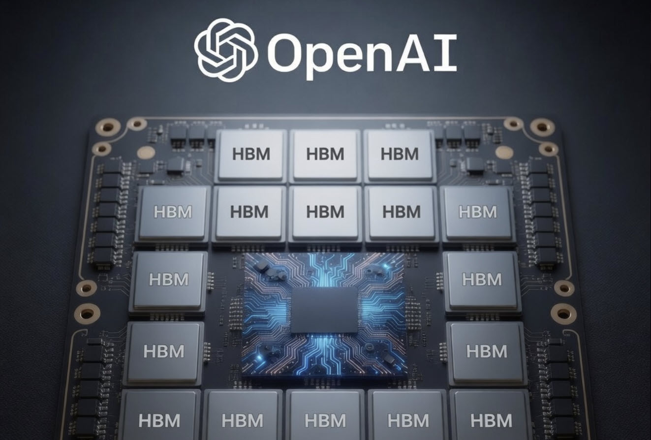
OpenAI has taken a bold step toward redefining AI hardware with a patent that outlines a custom chip architecture capable of stacking 20 high-bandwidth memory (HBM) modules, connected via an Intel EMIB-style bridge. This isn't just about raw performance—it's about how those stacks are integrated and managed to deliver efficiency gains that could shift the entire landscape for data center AI workloads.
The key innovation lies in how OpenAI is addressing one of the biggest bottlenecks in modern AI chips: memory bandwidth. Traditional designs struggle to keep up with the demands of large language models, where every extra terabyte per second of memory speed can translate into significant training and inference advantages. By stacking 20 HBM modules—each contributing its own bandwidth—OpenAI's design aims to push these limits further than any existing solution.
That’s the upside—here’s the catch. The EMIB-style bridges, which Intel pioneered for its own processors, are notoriously complex to implement. They require precise alignment of silicon layers and advanced packaging techniques that aren't trivial to scale. OpenAI's patent suggests they're tackling this by rethinking how these bridges are laid out on the chip, possibly using a modular approach that allows for more flexibility in manufacturing. If successful, this could set a new standard for how AI chips are built, but it also raises questions about whether the added complexity is worth the performance gains.
For enterprise buyers, the implications are significant. The ability to stack so many HBM modules suggests OpenAI is aiming for a future where AI chips aren't just faster, but more scalable in their memory capacity. This could be particularly appealing for organizations running large-scale language models or other AI workloads that demand both high bandwidth and low latency. However, the practical challenges of manufacturing such a design mean that adoption won't happen overnight. Buyers will need to weigh whether the potential performance boost justifies the risks of early adoption.
- Memory Stacks: 20 HBM modules, each contributing high-bandwidth memory capacity.
- Communication Bridges: Intel EMIB-style bridges for chip-to-chip connectivity.
- Performance Focus: Designed to address bottlenecks in AI training and inference workloads.
- Manufacturing Challenge: Advanced packaging techniques required, with potential scalability hurdles.
The patent doesn't provide specific benchmarks or release timelines, but it does offer a glimpse into OpenAI's long-term vision for AI hardware. If this architecture comes to market as described, it could push the industry toward more modular and scalable designs, where memory and compute are tightly integrated from the ground up. For now, the focus remains on whether OpenAI can overcome the engineering challenges without sacrificing efficiency or reliability.
Where things stand: This is still a patent, not a product, but it signals OpenAI's commitment to rethinking AI hardware at its core. Buyers should watch for updates on manufacturing progress and early benchmarks, but don't expect immediate availability.