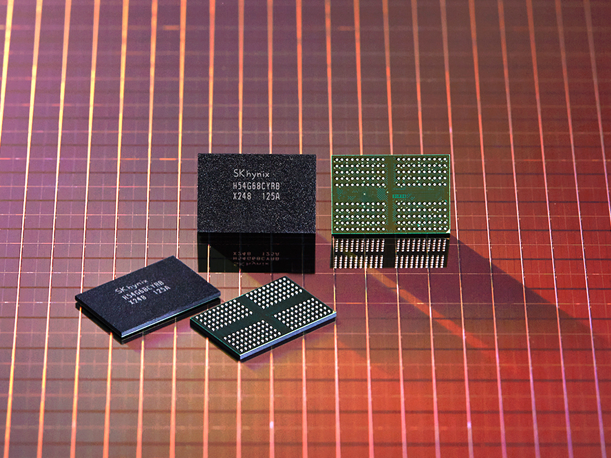
Samsung’s transition from a 24-month to a 12-month HBM development cycle is designed to address immediate market pressures, particularly in AI accelerators and high-end GPUs where memory bandwidth has become a limiting factor. The company is now prioritizing performance-per-watt improvements, a critical requirement for both data center operators and gaming enthusiasts.
- HBM stacks now support up to 16GB per package, enabling denser memory configurations.
- Thermal management remains a key challenge as stack heights increase, affecting power efficiency.
- Faster development cycles suggest upcoming HBM generations will focus on bandwidth and latency reductions.
- Market demand for AI workloads and high-refresh-rate gaming is driving the acceleration.
The shift comes as traditional DDR memory struggles to meet the needs of modern AI chips, which require the stacked architecture of HBM to handle larger datasets efficiently. While Samsung has not yet released new HBM products, industry analysts expect the compressed timeline to result in more frequent updates for GPUs and AI accelerators.
For end-users, this could mean quicker access to higher-bandwidth memory solutions, though pricing volatility may persist until supply chains stabilize. The focus on thermal efficiency also suggests that future generations will need to balance performance with power consumption—a growing concern as AI workloads become more energy-intensive.