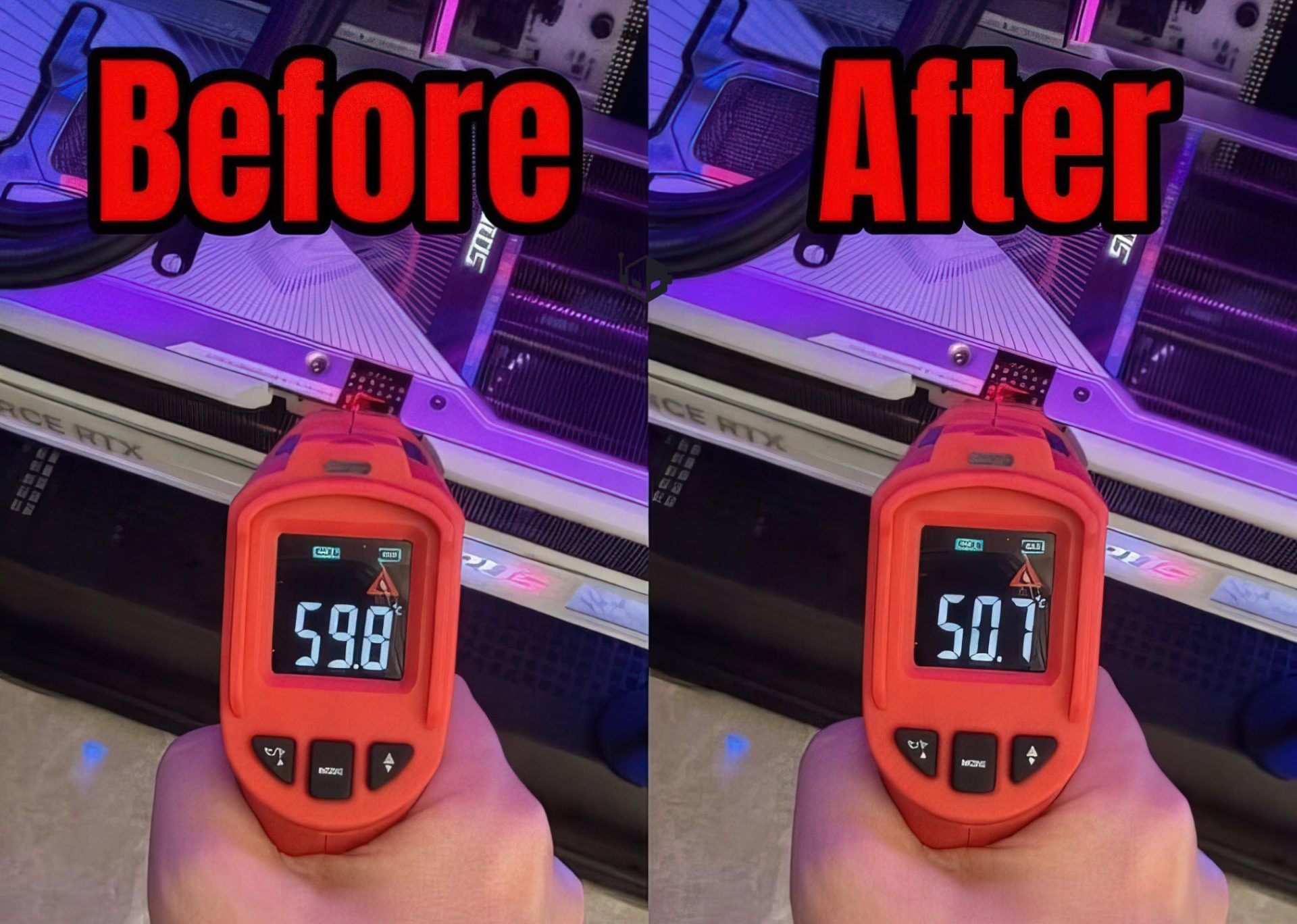
Samsung's semiconductor division has crossed a significant threshold with its 2nm chip manufacturing process, achieving 50% yield rates that could mark a turning point for the company's foundry business. This milestone comes as Samsung redirects its focus from earlier generations of 2nm technology to its more advanced SF2P iteration, setting the stage for next-generation AI processors and smartphone chips.
The achievement is notable because it represents a major improvement over Samsung's previous 3nm GAA process, which struggled to surpass 30% yields. That limitation had previously hindered Samsung's ability to compete effectively in high-volume markets like smartphones and data center chips. The shift to SF2P suggests the company is now positioning itself to challenge TSMC more aggressively in these segments.
What makes this development particularly interesting is its potential impact on two major product lines: AI processors and smartphone chips. Tesla's upcoming AI6 chip, part of a $16.5 billion deal with Samsung, is expected to be one of the first major products manufactured using SF2P. Meanwhile, Samsung's Exynos 2700, slated for next year, will likely leverage this process to support newer standards like LPDDR6 RAM and UFS 5.0 storage.
The timing also coincides with a broader industry trend of rising chip prices. Analysts estimate that memory demand from AI GPUs alone could push smartphone component costs up by $100 to $150 per unit this year, creating additional pressure on foundries like Samsung to optimize their manufacturing processes.

For consumers, the practical implications may not be immediately visible, but they will likely see faster, more efficient chips in next-generation devices. The shift to 2nm technology could also mean longer battery life and improved performance for smartphones and AI-powered devices. However, the real test for Samsung will be whether it can sustain these yields at scale while maintaining its profitability targets, with a goal of reaching break-even by 2027.
While Samsung's 50% yield rate is still below the industry standard of 80-90%, it represents a significant leap forward. The company's decision to prioritize SF2P over earlier iterations suggests confidence in its ability to refine this process and secure more high-profile customers, including major players like Tesla and Chinese cryptocurrency mining firms MicroBT and Canaan.
As Samsung continues to invest in its foundry capabilities, the next few years will be critical in determining whether it can carve out a meaningful share of the global chip market. For now, this milestone is a strong indicator that the company is moving beyond its early struggles with 2nm technology and positioning itself for a more competitive future.