Power users building AI workloads will soon face a critical choice: whether to adopt the next generation of DRAM before it becomes a locked-in platform. NEO Semiconductor has moved its 3D X-DRAM technology from concept to silicon, proving that existing 3D NAND infrastructure can deliver far greater density and thermal resilience than today’s JEDEC standards.
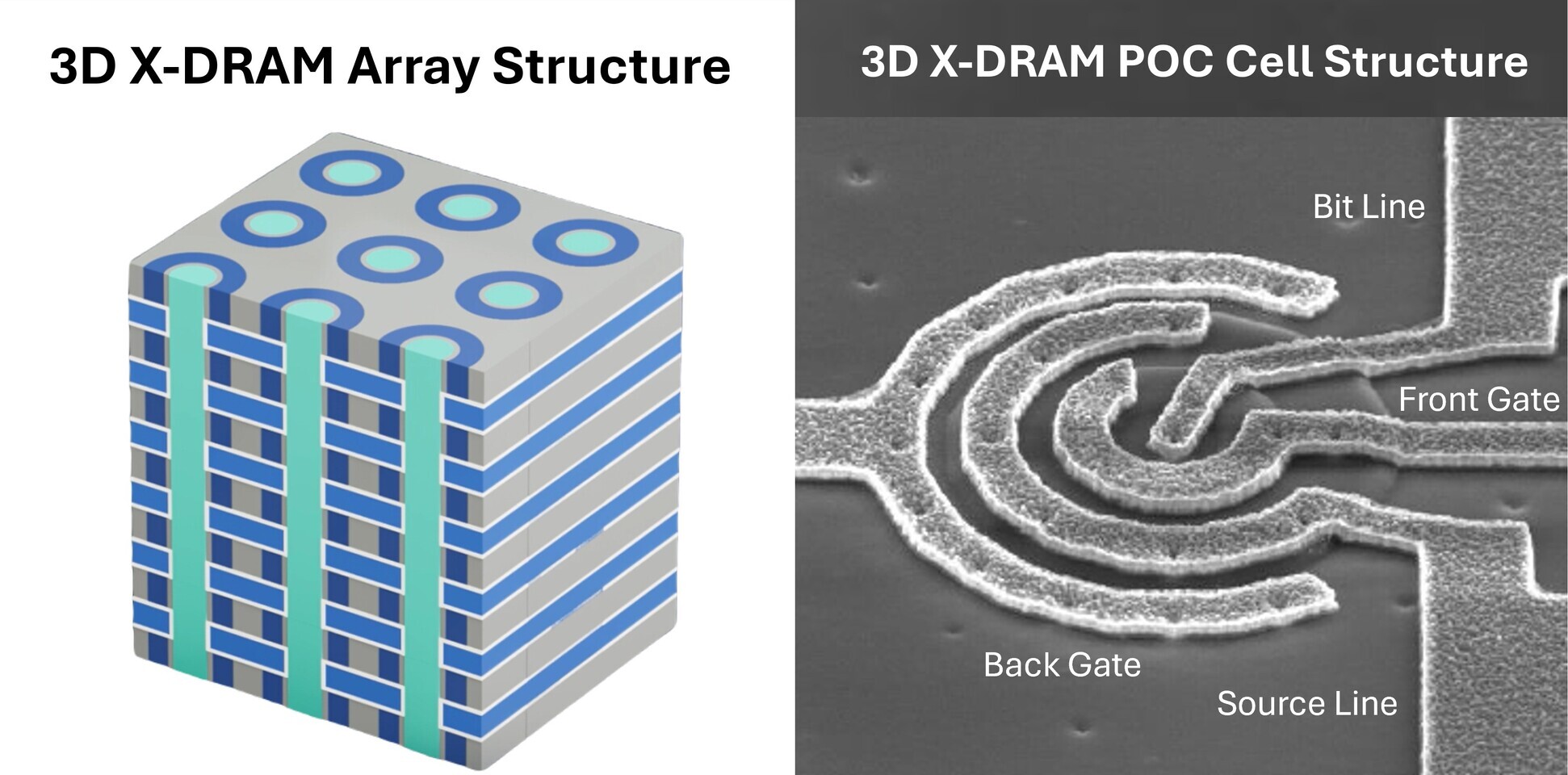
At the heart of the breakthrough is a test chip that operates at 85 °C with read/write latency under one second—more than fifteen times faster than current DRAM. Bit-line and word-line disturbances are suppressed beyond the one-second mark, while endurance reaches 10¹⁴ cycles, effectively eliminating refresh overhead for cold data. The architecture is built on mature 3D NAND processes already deployed in over 300-layer production, making it a direct drop-in for next-generation memory modules.
What power users gain
The immediate benefit for high-performance systems is clear: 8 GB modules can now be packed into far smaller footprints while consuming less power. For AI accelerators that push memory bandwidth to its limits, this means more cores on the same die without sacrificing speed or thermal headroom.
Yet the transition will not happen overnight. NEO’s roadmap hinges on two parallel tracks: a licensing model for foundries and a co-development partnership with leading memory manufacturers. The company is currently in active talks, but no official announcements have been made—leaving supply and pricing as the biggest unknowns.
Key details
- 8 GB capacity demonstrated on silicon test chips
- Read/write latency < 1 s at 85 °C (vs. 64 ms JEDEC standard)
- Bit-line & word-line disturbance > 1 s at 85 °C
- Endurance > 10¹⁴ cycles (effectively unlimited refresh cycles)
- Fabrication uses existing 3D NAND tools and materials
Development was a joint effort between NEO, the Industry-Academia Innovation School at National Yang Ming Chiao Tung University, and the NIAR-TSRI research institute in Taiwan. The POC passed rigorous electrical and reliability tests under real process conditions, confirming that the architecture can be scaled without new equipment.
Why this matters now
For power users, the shift to 3D X-DRAM represents more than a performance bump—it marks the beginning of a platform lock-in. Once adopted in AI hardware, the technology will set new benchmarks for memory density and thermal efficiency that current designs cannot match.
But adoption is not automatic. The industry must first agree on standards, and foundries must commit to volume production. NEO’s CEO, Andy Hsu, has signaled a licensing approach rather than in-house fabrication, which could accelerate time-to-market but also tie system designers to a single supplier ecosystem.
What to watch next
The most important change is that 3D X-DRAM is no longer theoretical. It is a proven architecture, ready for array-level implementation and multi-layer test chips. The question now is how quickly the industry will move from POC to production—and whether power users will be able to upgrade without being locked into a single memory platform.
NEO plans deeper engagement with global memory companies in the coming months, but no commercial samples or price points have been announced. For those building next-generation AI systems, the window for early adoption is opening—but the supply chain and pricing will decide who gets to step through first.