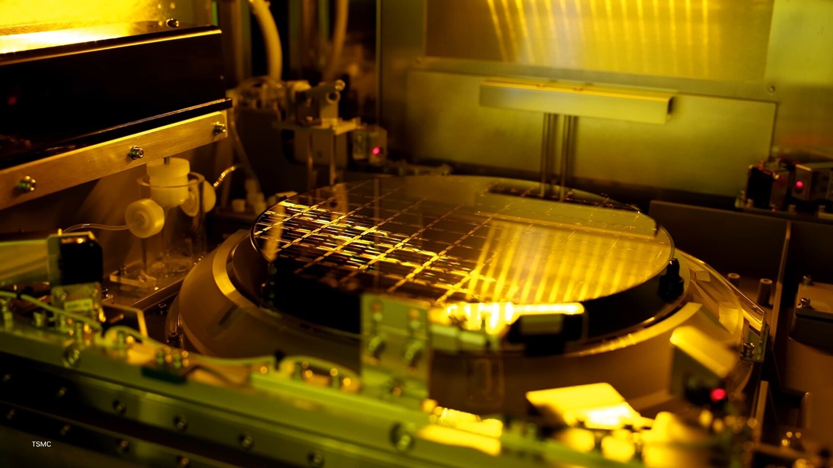
Monday, June 1st 2026 NVIDIA and TSMC Bring AI Into Fabs to Advance Semiconductor Design and Manufacturing Press Release by GFreeman Today, 02:27 Discuss (0 ) NVIDIA today announced that TSMC, the world's leading semiconductor company, is using NVIDIA accelerated computing and AI to advance semiconductor design and manufacturing. As chips move to more advanced nodes, bringing them from design to high-volume production has become one of the world's most complex computing challenges. Computational lithography, transistor simulation, process control and wafer inspection now require massive-scale simulation and real-time optimization, and AI systems that can provide support across physics, images and other applications. TSMC is using NVIDIA technologies to accelerate this transformation, applying accelerated computing and AI across the semiconductor design and manufacturing lifecycle to improve turnaround time, energy efficiency, yield and operational productivity in advanced fabs. "NVIDIA and TSMC have worked together for nearly three decades to push the limits of computing," said Jensen Huang, founder and CEO of NVIDIA. "TSMC is bringing NVIDIA AI and accelerated computing into the fab itself, tackling some of the world's most complex design and manufacturing challenges with simulation, optimization and AI to improve speed, efficiency and yield for the next generation of chips." "TSMC and NVIDIA have built a long-standing partnership rooted in advancing the technologies that make the next generation of computing possible," said C.C. Wei, chairman and CEO of TSMC. "By using NVIDIA accelerated computing and AI across fab operations optimization, lithography, process control and inspection, TSMC is strengthening our technology leadership and manufacturing excellence to support our customers' future products and success." TSMC Accelerates Processes With NVIDIA CUDA-X Libraries and AI Advanced semiconductor design and manufacturing require massive computational workloads and highly coordinated fab operations, spanning chip-design transfer, transistor modeling, process control and fab productivity. TSMC is using NVIDIA CUDA-X libraries and AI models to accelerate these workloads on NVIDIA GPUs:Computational lithography: TSMC is using NVIDIA cuLitho, a GPU-accelerated library for lithography - a printing method for chip mask design. This technology delivers a 20-50% improvement in cost effectiveness or cycle time compared with CPU-based computational lithography, while maintaining the same cost of ownership.Transistor, equipment and process simulation: TSMC is using NVIDIA cuEST, a GPU-accelerated electronic structure simulation library for 50x faster chemistry simulations, on average, for semiconductor material design.Advanced process control: TSMC is using the NVIDIA cuML machine learning library to accelerate large-scale analytics on NVIDIA GPUs. This lets TSMC speed algorithms and distill hundreds of thousands of process parameters spanning thousands of steps as precision inputs for machine learning models - making significant reduction in process variation.Fab operations optimization: GPU-accelerated scheduling computation using CUDA has led to notable improvements in fab productivity with NVIDIA H200 GPUs. By harnessing CUDA-powered computation on NVIDIA H200 GPUs, TSMC has enhanced its capability to manage complex constraints, thereby streamlining production paths and maximizing fab productivity.TSMC Advances Defect Inspection With NVIDIA Metropolis and AI Models As chips become more advanced, even the smallest defects can affect quality and yield, making faster and more accurate inspection essential to semiconductor design and manufacturing. TSMC is using the NVIDIA Metropolis platform and NVIDIA TAO Toolkit to improve advanced defect classification. Using vision AI, TSMC has improved detection of defects at nanometer scale. These capabilities help TSMC improve quality inspection while reducing the need for repeated labeling and retraining as process conditions, inspection tools and defect types change. TSMC Taps NVIDIA Omniverse to Build FabTwin Advanced semiconductor fabs are among the most complex fabs ever built, requiring precise coordination across tools, materials, robots, humans and facility systems. TSMC is exploring NVIDIA Omniverse libraries to build FabTwin, a virtual fab environment for evaluating process tool layouts and related simulation workflows. By testing design scenarios digitally before physical implementation, TSMC can compare complex configurations more flexibly and identify potential constraints earlier. This virtual-first approach vastly improves planning efficiency and accelerates critical decision-making before any physical or capital commitments are made. Source: NVIDIA Related News Tags: AI Jensen Huang Manufacturing ML NVIDIA Omniverse Semiconductor TSMC Jul 23rd 2025 DDR6 Memory Arrives in 2027 with 8,800-17,600 MT/s Speeds (196) Jan 16th 2026 NVIDIA Reportedly Ends GeForce RTX 5070 Ti Production, RTX 5060 Ti 16 GB Next (210) Sep 18th 2025 NVIDIA Buys $5B Worth of Intel, RTX iGPUs Coming to x86, Shares up 25% (256) Mar 30th 2026 NVIDIA Readies Rubin-based GeForce RTX 60-series with Massive RT Performance Gains (162) Sep 10th 2025 NVIDIA GeForce RTX 50-Series SUPER GPUs Could Arrive at CES 2026 (69) Dec 31st 2025 Leaks Predict $5000 RTX 5090 GPUs in 2026 Thanks to AI Industry Demand (124) Sep 3rd 2025 NVIDIA Discrete GPU Market Share Dominance Expands to 94%, Notes Report (237) Jul 29th 2025 NVIDIA to Debut GeForce RTX 50-series SUPER GPUs by Christmas (112) Sep 29th 2025 March-April Release of NVIDIA GeForce RTX 50-series SUPER Lineup, Possible CES Reveal (73) Mar 16th 2026 NVIDIA Unveils DLSS 5 with Real-Time Neural Rendering (305) Add your own on NVIDIA and TSMC Bring AI Into Fabs to Advance Semiconductor Design and Manufacturing There are no yet.