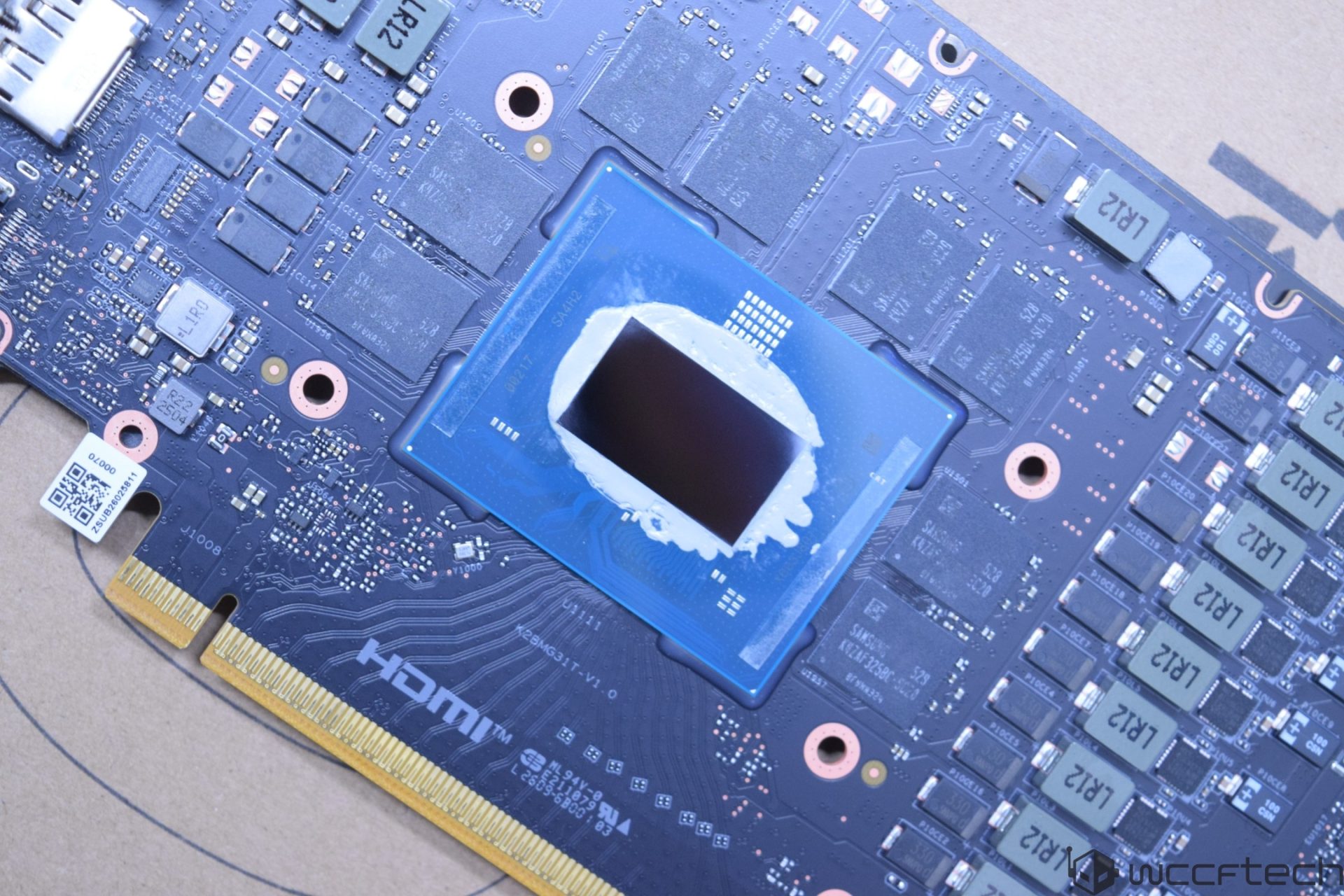
The race to push semiconductor technology to its limits just took a significant step forward. NVIDIA’s annual GTC conference, set to begin in San Jose on March 15, is poised to reveal one of the most ambitious hardware projects in recent memory: the Feynman AI accelerator. What makes this announcement particularly intriguing is that Feynman isn’t just another incremental upgrade—it may be the first chip in the world built on TSMC’s 1.6nm A16 process, a leap that could redefine the boundaries of performance, power efficiency, and even manufacturing complexity.
This isn’t just about shrinking transistors further. The A16 node introduces Super Power Rail (SPR), a technology designed to optimize power delivery at an unprecedented scale. TSMC has positioned itself as the sole early adopter for this process, with NVIDIA as its first and possibly only customer during the initial high-volume manufacturing phase. The implication is clear: Feynman could become a cornerstone for next-generation AI workloads, offering densities and efficiencies that today’s 4nm and 3nm chips simply can’t match.
A Hybrid Approach to AI Acceleration
But Feynman’s potential doesn’t stop at the foundry. There are strong indications that NVIDIA may integrate Groq’s LPU (Language Processing Unit) architecture into its design. While details remain scarce, this could represent a strategic pivot toward low-latency, high-throughput computing—an area where Groq has carved out a niche with its specialized hardware. The integration would likely follow a hybrid bonding approach, similar to AMD’s X3D processors, where multiple dies are stacked vertically to improve bandwidth and reduce latency. Such a design would be a major engineering challenge, but if successful, it could deliver AI performance that bridges the gap between traditional GPUs and custom accelerators.
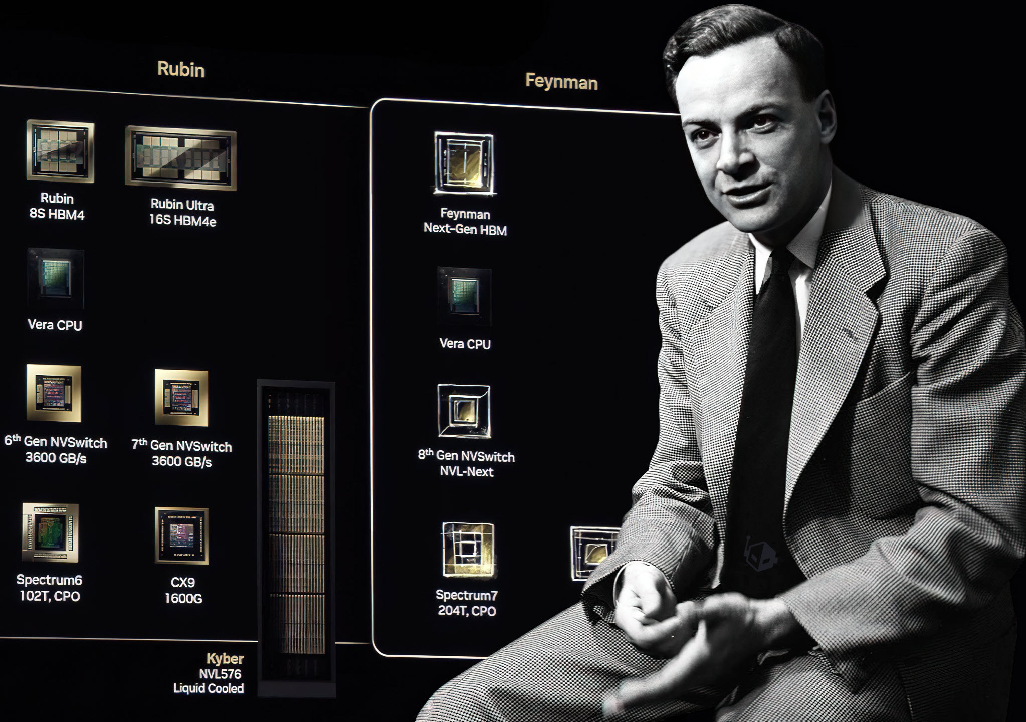
The comparison to NVIDIA’s Vera Rubin (the codename for its Blackwell architecture) is apt. When Rubin was unveiled, it signaled a shift toward massive-scale AI clusters with record-breaking memory and compute capabilities. Feynman appears to be the next evolution—one that may prioritize agility and efficiency over sheer scale. If production ramps up as anticipated, with customer shipments possible by 2029–2030, the implications for industries reliant on AI—from generative models to real-time analytics—could be profound.
Why This Matters
For AI researchers and enterprises, the arrival of 1.6nm chips means several critical advantages
- Unprecedented Efficiency: Smaller nodes translate to lower power consumption and higher transistor density, enabling more complex AI models to run on less energy.
- Performance Leaps: The combination of SPR and potential LPU integration could result in sub-nanosecond latency for certain workloads, a game-changer for applications like autonomous systems or financial modeling.
- First-Mover Advantage: NVIDIA’s early adoption of A16 positions it at the forefront of semiconductor innovation, potentially influencing competitors to accelerate their own roadmaps.
Yet, the path to Feynman won’t be without challenges. The 1.6nm process demands significant architectural revisions, and integrating Groq’s LPUs adds another layer of complexity. If NVIDIA can pull this off, however, it could set a new standard for what’s possible in AI hardware—one that blurs the line between general-purpose acceleration and specialized, ultra-efficient computing.
The stage is set for GTC 2026 to be more than just another keynote. It may well be the moment when the next decade of AI infrastructure begins to take shape.