Next-generation AI chips are pushing the limits of what traditional silicon can handle—so a new material platform may be needed to keep up. Silicon carbide (SiC), long used in high-power electronics, is emerging as a potential foundation for advanced packaging that could support larger, more power-dense AI systems by the end of this decade.
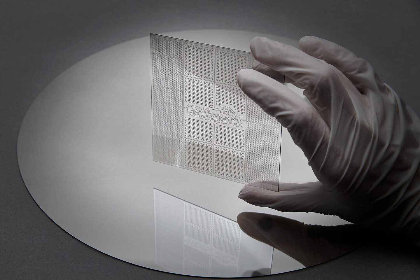
Wolfspeed’s 300 mm SiC technology platform is designed to combine the material’s superior thermal conductivity and mechanical strength with industry-standard manufacturing processes. The goal is to create substrates capable of handling the increasing size, power density, and complexity of AI and high-performance computing (HPC) packages without requiring entirely new fabrication infrastructure.
What might change—and what won’t
The shift toward SiC could address several key bottlenecks in current packaging designs. Traditional silicon-based interposers struggle with thermal management as power demands rise, often leading to performance throttling or reliability issues. SiC, by contrast, conducts heat more efficiently and maintains structural integrity under higher temperatures, which could help sustain AI workloads that require sustained high performance.
However, the transition won’t be seamless. While 300 mm SiC wafers align with existing semiconductor manufacturing equipment, integrating them into complex multi-chip packages—especially those combining silicon and SiC layers—remains unproven at scale. Wolfspeed is working with foundries, OSATs (outsourced semiconductor assembly and test providers), and system architects to validate performance, reliability, and cost scalability before widespread adoption.
Key considerations for AI data center designs
- Thermal performance: SiC’s higher thermal conductivity could reduce cooling requirements in dense packages, potentially lowering operational costs.
- Package size and complexity: The 300 mm format allows for larger interposers and heat spreaders, supporting the trend toward bigger, more integrated AI modules.
- Manufacturing compatibility: Existing 300 mm fabrication lines can process SiC wafers, avoiding the need for new capital expenditures—at least in theory.
The biggest uncertainty is whether SiC can deliver these benefits without introducing new manufacturing challenges. Early collaborations suggest it’s feasible, but real-world validation will take time.
For now, the focus remains on proving that SiC substrates can meet the demands of next-generation AI chips—without derailing the cost and efficiency gains that have driven silicon packaging forward for decades.