Tesla is doubling down on custom silicon, positioning itself as a potential disruptor in the semiconductor industry. The automaker’s latest moves suggest an aggressive push to dominate both volume production and performance metrics, potentially reshaping how AI-driven systems are built for vehicles and data centers.
The centerpiece of this strategy is the AI5 chip, which Tesla claims will deliver Hopper-class performance with a single die or Blackwell-level performance when paired with two dies. This represents a significant leap in efficiency, particularly for autonomous driving workloads where compute demands are growing exponentially. The company’s goal isn’t just to match competitors but to undercut them on cost, creating a platform that could accelerate the mainstream adoption of its Full Self-Driving (FSD) technology.
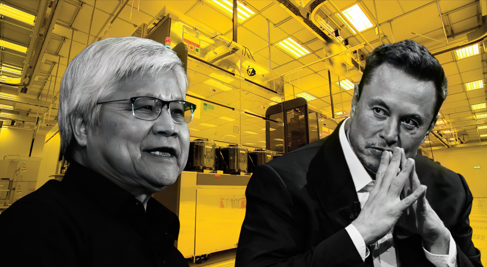
Supporting this ambition is the revival of Tesla’s Dojo3 supercomputer project, which was previously paused due to challenges in talent retention and strategic pivots. The return of Dojo3 signals a renewed focus on vertical integration, allowing Tesla to control both the silicon design and the systems that will run it—from vehicles to data center deployments. This approach mirrors NVIDIA’s playbook but with a key difference: scale.
Industry observers note that mastering semiconductor manufacturing is no small feat, requiring decades of experience across design, verification, and mass production. Tesla’s ambitions hinge on its ability to execute flawlessly at every stage, from the 2nm process node—where leading-edge foundries like TSMC are already operating—to the stability and reliability of its own silicon. If successful, this could give Tesla an unassailable lead in both performance and cost per unit, particularly as FSD becomes a standard feature rather than a premium offering.
The AI5 chip is designed to be the highest-volume product in Tesla’s lineup, with plans to extend the family up to AI9 chips. The company has set an aggressive nine-month cadence for new chip generations, a pace that rivals NVIDIA’s own development cycles. This rapid iteration could further solidify Tesla’s position if it can maintain both performance gains and cost efficiency.
For consumers and businesses relying on Tesla’s FSD ecosystem, the implications are clear: lower costs, more capable hardware, and potentially faster innovation in autonomous driving. However, the path to execution remains uncertain. While Tesla has demonstrated an ability to innovate quickly—from battery technology to software stacks—the challenges of semiconductor manufacturing are profound, spanning everything from process engineering to yield optimization.
Key specs for the AI5 chip include
- Performance: Targets Hopper-class performance with a single die or Blackwell-level performance with two dies.
- Cost Efficiency: Designed to offer significant price advantages over competing architectures, particularly in high-volume production scenarios.
- Process Node: Built on advanced 2nm technology, aligning with the most cutting-edge foundries.
- Use Cases: Optimized for autonomous driving workloads and AI acceleration, with potential applications in data center deployments via Dojo3.
The AI5 chip’s design reflects Tesla’s focus on unifying its silicon stack across vehicles and data centers. This integration could streamline development cycles and reduce dependencies on external suppliers, further reinforcing Tesla’s vertical control over its technology roadmap.
While the company has not yet confirmed availability or pricing for the AI5 chip, industry insiders suggest that early deployments in FSD systems could begin as soon as 2026, depending on progress in manufacturing ramp-up. If Tesla can deliver on its promises, it may force competitors to rethink their strategies—not just in performance, but in how they approach cost and scale.