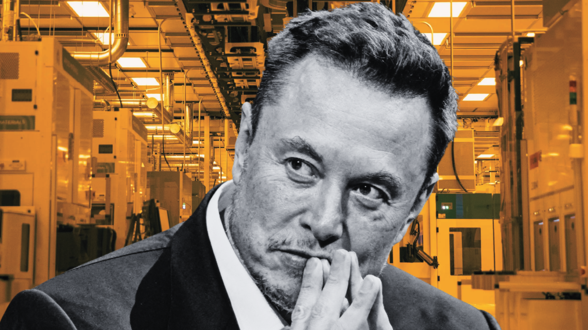
A developer working late on a custom AI accelerator suddenly hits a wall: the chip they need isn’t just delayed—it’s stuck in a global queue that stretches for months. That bottleneck isn’t theoretical anymore; it’s a daily reality for companies chasing next-gen silicon, and Tesla is now betting its future on cracking it open.
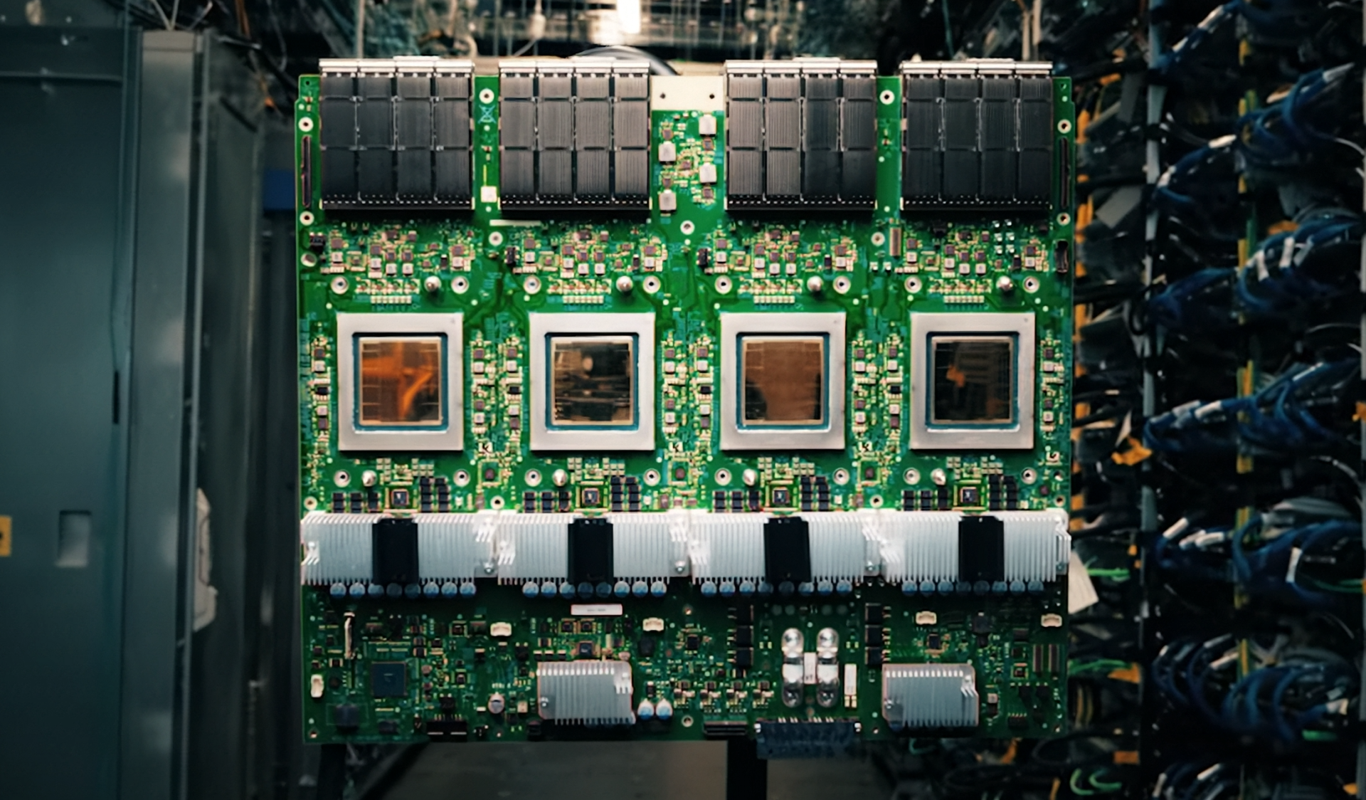
Next week, the company will reveal the architecture of its so-called TeraFab—a facility designed to churn out 100 billion to 200 billion chips per year. If realized, that output would dwarf even TSMC’s most advanced fabs, but the devil lies in the details: no cleanroom, no traditional foundry model, and a reliance on partnerships that blur the line between capital infusion and co-manufacturing.
Specs at a glance
- Targeted output: 100–200 billion chips per year
- Process node: 2 nm (confirmed)
- Cleanroom: None—reportedly ruled out in favor of modular or licensed lines
- Partnership model: Likely based on licensing deals with Intel Foundry and/or TSMC for capacity booking
The TeraFab isn’t just about volume; it’s a gamble that the U.S. can leapfrog decades of semiconductor infrastructure by leveraging Tesla’s vertical integration and deep pockets. The 2 nm node is the headline number, but the real innovation—or risk—is in how the fab avoids the $20B+ capital expenditure of a greenfield cleanroom. Early indications point to a hybrid model: Tesla would effectively pre-pay for production lines at existing foundries, then resell capacity to itself and third parties under a single roof.
Who it’s for—and who it leaves behind
This isn’t just about Tesla’s Dojo AI chips or its rumored Blackwell competitor. The project targets any company willing to lock in long-term demand, but the tradeoff is stark: no flexibility, no leading-edge R&D, and a heavy upfront commitment. Startups and niche players may find the model too rigid; established giants like NVIDIA or AMD could still out-innovate on process nodes while using Tesla’s capacity for volume.
The catch
That’s the upside—here’s the catch. Without a cleanroom, yield and control become shared risks with partners, not Tesla alone. Intel Foundry has shown openness to such deals, but TSMC remains cautious about ceding market share. Meanwhile, the U.S. government’s chip subsidies could make this model more viable overnight, yet no one knows if the paperwork will align with the timeline.
The most critical change isn’t the 2 nm node—it’s the idea that a non-traditional player can bypass the entire foundry ecosystem by acting as a de facto capacity aggregator. If it works, semiconductor supply chains will never look the same. If it fails, Tesla may have just taught the industry how not to build a fab.