The race to dominate AI memory is no longer just about raw speed. It’s about stacking layers of silicon with surgical precision, bonding them so tightly that data moves faster than ever before—but without the numbers to prove it can be done at scale.
SK hynix has quietly verified a 12-die hybrid bonded HBM stack, a configuration that could push bandwidth beyond 6 terabytes per second. This is not just an incremental upgrade from HBM3; it’s a leap in architecture. The company’s approach bonds dies vertically, eliminating the bottlenecks of traditional horizontal stacking. For AI workloads, this means less latency and more data moving through memory at once—critical for training models that demand petabytes of information.
But performance alone doesn’t guarantee adoption. The industry’s focus now shifts to yield—a metric SK hynix has not disclosed. If the stack can be produced reliably, it could redefine how data centers operate. A single HBM4 module might replace multiple DDR5 channels, slashing power consumption and accelerating AI training. Yet without knowing how many of these stacks will pass quality checks, buyers face a gamble: cutting-edge performance or unproven reliability?
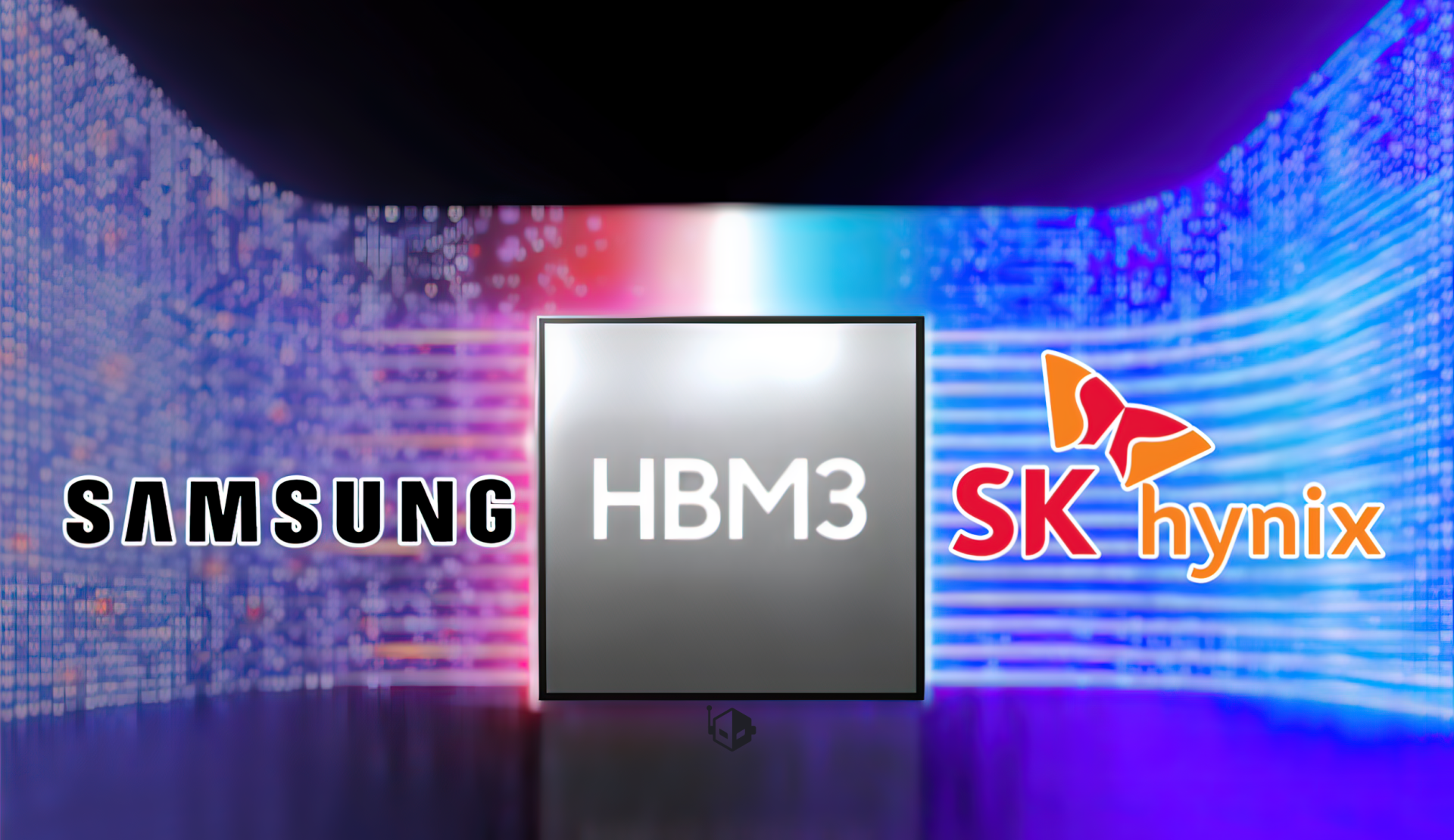
Competitors are not standing still. Samsung and Micron are also advancing their own HBM designs, but the transition from lab to production remains fraught with challenges. The industry is at a crossroads—where theoretical gains clash with practical constraints. For AI operators, the real question isn’t whether HBM4 will deliver speedups, but whether it can be deployed without crippling costs.
The race for AI memory is silent now, with no benchmarks or public announcements to mark its progress. The next phase begins when yield data emerges—when the promise of 6 terabytes per second moves from verification to real-world deployment. Until then, the industry must tread carefully between hype and hard numbers.