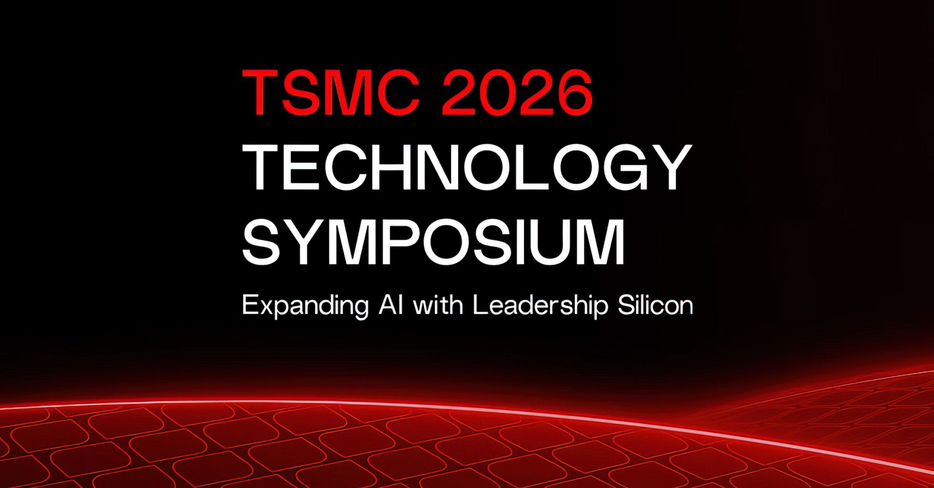
Semiconductor manufacturers are facing a critical choice: whether to adopt the most advanced but prohibitively expensive extreme ultraviolet (EUV) lithography tools or develop alternatives that, while less precise, offer significant cost savings. TSMC's upcoming A13 and A12 nodes, slated for production in 2029, represent a strategic pivot away from ASML's highest-tier EUV systems, potentially reshaping the industry's cost dynamics.
TSMC's decision to sidestep ASML's most expensive tools suggests a deliberate effort to balance performance and affordability. While the A13 node at 1.3 nanometers will still leverage EUV technology, it will avoid the more advanced and costly systems that have become a bottleneck for leading-edge chip production. The A12 node, targeting 1.2 nanometers, is expected to push the boundaries of what's feasible without relying on ASML's priciest equipment.
This shift could have profound implications for both TSMC and its customers. For TSMC, it means avoiding the substantial capital expenditure required to deploy the latest EUV tools while still delivering cutting-edge performance. For customers, particularly those in high-volume markets like smartphones and data centers, this could translate into more affordable chips without sacrificing performance.
However, this strategy is not without its challenges. The A13 node will still require advanced EUV technology, albeit at a lower cost than the most recent iterations. TSMC's engineers will need to innovate in other areas, such as materials and process integration, to compensate for the lack of ASML's highest-tier tools. Additionally, the industry must ensure that these nodes can meet the demands of increasingly complex chip designs, particularly for AI and high-performance computing.
- A13 Node (1.3nm): Uses EUV but avoids ASML's most expensive tools; targets 2029 production.
- A12 Node (1.2nm): Pushes the limits of current technology without relying on ASML's priciest equipment; also slated for 2029.
The practical impact of this roadmap will be felt most acutely in markets where cost is a critical factor, such as consumer electronics and data center infrastructure. TSMC's ability to deliver high-performance chips at competitive prices could give it an edge over competitors, but the long-term sustainability of these nodes remains to be seen.
For creators and engineers, this development signals a potential shift in how chips are designed and manufactured. The focus on cost efficiency may lead to more innovative approaches in chip architecture, with an emphasis on optimizing performance within tighter constraints. This could accelerate advancements in AI and high-performance computing, as manufacturers seek to maximize the capabilities of these nodes.
What to watch: TSMC's ability to deliver on its 2029 roadmap will be a key indicator of whether this strategy can succeed without sacrificing performance. The industry will also be closely monitoring the evolution of EUV technology and how it impacts the cost and feasibility of future process nodes.