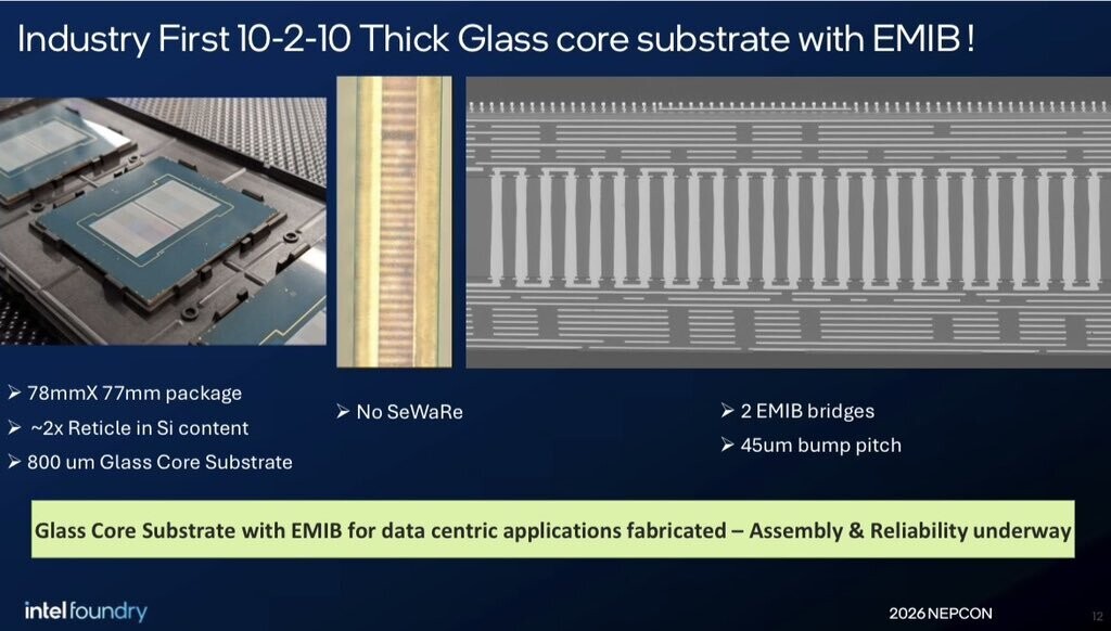
Intel has introduced a radical new packaging architecture at NEPCON Japan 2026 that could reshape the future of AI and high-performance computing (HPC) accelerators. The company’s glass core substrate—measuring 78×77 millimeters—marks a departure from traditional organic substrates, offering twice the silicon area capacity (1,716 mm²) while eliminating a manufacturing defect known as SeWaRe (surface and edge warpage-related micro-cracking).
At the heart of the innovation is a 10-2-10 layer stack: 10 redistribution layers (RDLs) on the top and bottom for signal routing, with a two-layer glass core (800 µm thick) sandwiched between. This design allows for embedded metal layers for through-glass-vias (TGVs) or power/ground planes, while the symmetric build-up layers simplify integration with motherboards. The substrate also features industry-leading 45 µm bump pitches, enabling denser interconnects without compromising reliability.
Perhaps most critically, the technology integrates EMIB (Embedded Multi-die Interconnect Bridge) bridges, enabling multi-chip modules (MCMs) where smaller dies can be interconnected directly on the glass substrate. This approach not only reduces thermal bottlenecks but also improves signal integrity—a key advantage for tightly coupled AI and HPC workloads.
Manufacturing challenges have historically plagued glass substrates, particularly micro-cracking during dicing and assembly. Intel claims to have overcome this through material science or process refinements, ensuring the substrates remain intact even under high-stress conditions. The result is a package that offers better heat resistance, reduced warping, and enhanced electrical isolation compared to conventional organic substrates.
**Key Specifications**
- Substrate Dimensions: 78×77 mm (supporting up to 1,716 mm² of silicon area)
- Layer Configuration: 10-2-10 (10 RDLs top, 2-layer glass core, 10 RDLs bottom)
- Glass Core Thickness: 800 µm (0.8 mm), with embedded metal layers for TGVs or power/ground planes
- Bump Pitch: 45 µm (0.045 mm), enabling finer interconnects
- EMIB Integration: Two EMIB bridges for multi-chip module packaging
- Manufacturing Achievement: Elimination of SeWaRe (micro-cracking) during production
The implications for AI and HPC are substantial. Traditional organic substrates struggle with signal delays and thermal management as chip densities increase. Glass, by contrast, provides superior thermal conductivity and electrical isolation, allowing for higher interconnect densities without performance degradation. This could lead to more efficient cooling solutions and reduced power consumption in next-generation accelerators.
While Intel has not confirmed whether the technology will be licensed externally or retained in-house, the development underscores the company’s push toward advanced packaging solutions. Competitors in the space remain limited, making this a potential differentiator for Intel’s roadmap in AI and HPC markets.