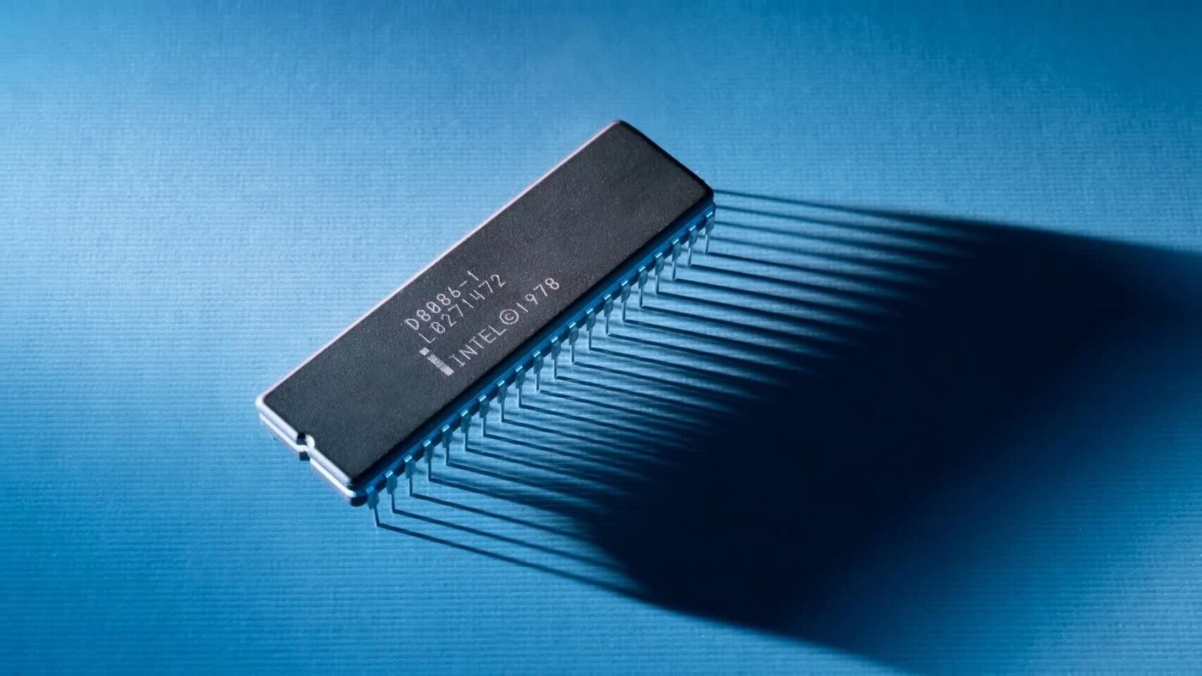
NVIDIA is breaking new ground in AI chip manufacturing by distributing production of its Feynman architecture across two foundries—TSMC and Intel—while adopting advanced packaging techniques. The strategy, which allocates a quarter of Feynman’s output to Intel’s emerging 18A and 14A processes, reflects a broader industry trend toward supply chain diversification. For Intel, this partnership represents a critical validation of its foundry capabilities, particularly in high-performance computing. Meanwhile, NVIDIA’s cautious approach—outsourcing only the I/O die to Intel—minimizes risk while testing the waters for future collaborations.
At a glance
- Dual-foundry production: Feynman chips will split between TSMC (75%) and Intel Foundry (25%), with Intel handling the I/O die.
- Process nodes: Intel’s 18A and 14A nodes will be used, with 14A likely for higher-volume production.
- Advanced packaging: Intel’s EMIB (Embedded Multi-die Interconnect Bridge) will integrate Feynman’s dies for improved performance.
- Cost and risk management: NVIDIA’s partial shift to Intel avoids over-reliance on TSMC while mitigating yield risks.
- Broader industry impact: The move signals a potential turning point for Intel’s foundry division, which has struggled to attract major customers.
- Geopolitical hedge: Diversification aligns with concerns over Taiwan’s stability and TSMC’s dominance in AI chip production.
- Potential for gaming GPUs: Intel’s packaging and process nodes could extend to NVIDIA’s non-AI products in the future.
Why this matters
Intel’s foundry division has spent years playing catch-up to TSMC, but recent breakthroughs—particularly in advanced packaging and 18A/14A processes—have positioned it as a viable alternative. For NVIDIA, the partnership is a pragmatic step: TSMC’s AI-focused capacity is stretched thin, and hyperscalers are struggling to secure slots. By outsourcing a portion of Feynman to Intel, NVIDIA ensures continuity without betting the farm on a single supplier. The 25% allocation to Intel also serves as a proof-of-concept, with potential to scale if yields and costs align with expectations.
The decision carries implications beyond NVIDIA. AMD and Qualcomm have already begun exploring dual-foundry strategies with Samsung and TSMC, but Intel’s entry into the AI chip market could force TSMC to accelerate innovation or risk losing ground. For Intel, landing NVIDIA—even for a single die—is a major coup, demonstrating that its foundry can handle high-performance workloads. The use of EMIB packaging, in particular, highlights Intel’s focus on advanced interconnect solutions, a critical enabler for next-generation AI and HPC designs.
Looking ahead
The Feynman split is just the beginning. With TSMC’s dominance under scrutiny, other fabless companies may follow NVIDIA’s lead, creating a more competitive foundry ecosystem. Intel’s ability to deliver on its promises—especially in yield and cost—will determine how quickly this shift accelerates. For now, NVIDIA’s measured approach balances risk and opportunity, setting a template for how AI hardware giants can navigate a fragmented supply chain. The real question is whether Intel can turn this partnership into a long-term relationship—or if it remains a one-off experiment in an industry still heavily reliant on TSMC.
As the AI boom continues, the stakes for foundry diversification grow. NVIDIA’s move underscores a simple truth: in an era of geopolitical tensions and exploding demand, no single player can afford to have all its chips in one basket.