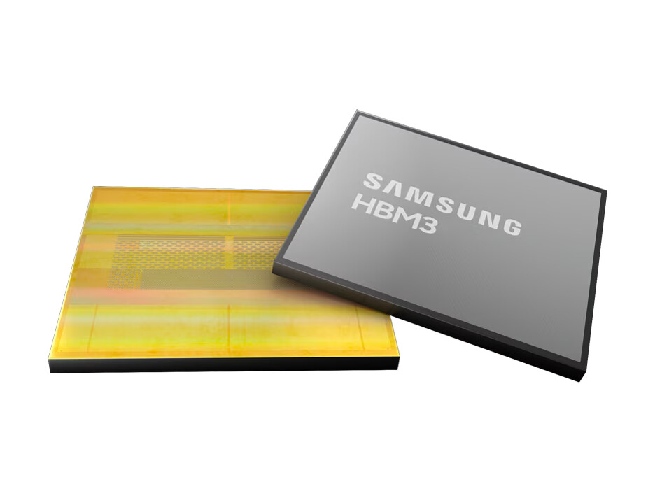
Samsung is quietly advancing one of the most ambitious memory projects in semiconductor history, pushing logic dies for high-bandwidth memory (HBM) to a 2 nanometer process—a leap that could redefine performance benchmarks for AI accelerators and data centers. While details remain scarce, industry insiders suggest this isn't just another incremental upgrade; it's a strategic pivot toward custom, application-specific HBM designs tailored for next-generation computing demands.
The South Korean giant's System LSI Business Division, which established a dedicated team last year to focus on custom system-on-chip (SoC) solutions, is now applying that expertise to memory. Unlike traditional foundry models where customers adapt to predefined nodes, Samsung appears to be reversing the equation—offering bespoke logic dies optimized for specific workloads, from AI inference engines to high-performance GPUs. This approach mirrors trends seen in CPU and GPU design but extends them into the memory ecosystem, an area historically dominated by standardized architectures.
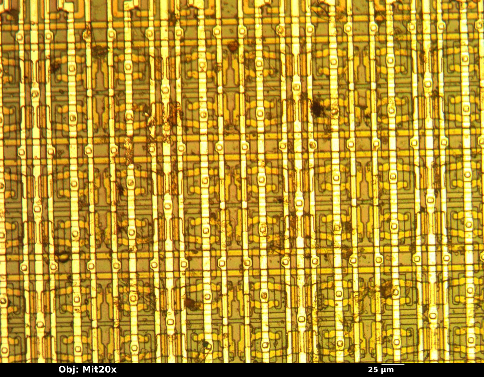
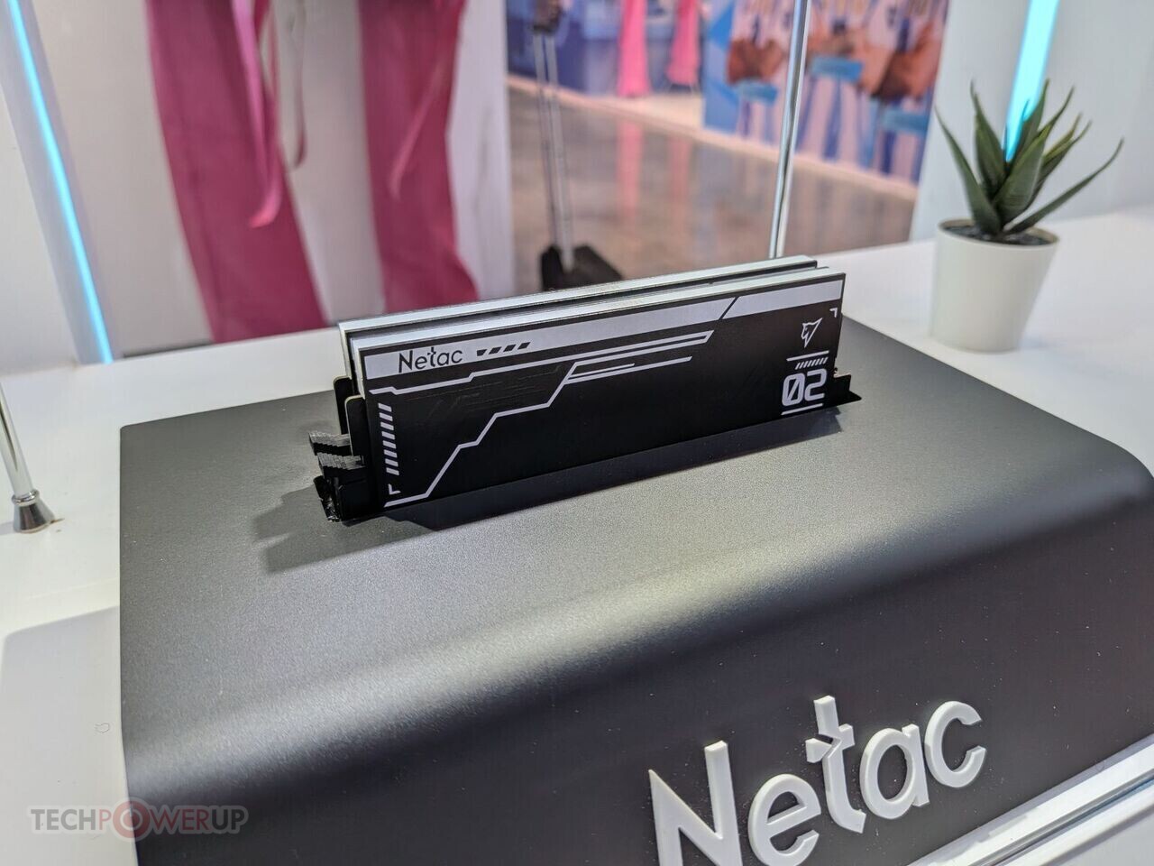
Currently, Samsung's sixth-generation HBM (HBM4) is built on a 4 nm process node, likely derived from its SF4 family, which has already demonstrated strong adoption in AI and data center applications. But the push to 2 nm— rumored to leverage either the company's advanced foundry nodes (SF2 or SF2P) — signals a shift toward even more aggressive performance targets. The 2 nm node, if realized, would sit at the bleeding edge of semiconductor fabrication, competing with the most cutting-edge logic processes used in today's AI chips and GPUs.
Why does this matter? HBM has become the backbone of ultra-high-performance computing, especially for AI accelerators where memory bandwidth is as critical as raw compute power. Traditional DRAM struggles to keep up with the demands of modern neural networks, leading to a growing reliance on stacked, high-bandwidth modules that can deliver terabytes per second of data throughput. Samsung's move to 2 nm logic dies suggests it's aiming to squeeze even more performance out of these modules—reducing latency, increasing density, and potentially lowering power consumption in the process.
Industry analysts speculate that the first fruits of this R&D will appear in enterprise AI systems, possibly as early as post-2027, once HBM4E (the seventh generation) matures. The timing aligns with projections for a surge in demand from data centers and AI workloads, where every cycle saved in memory access can translate to significant efficiency gains. For now, the focus remains on refining the technology, but the implications for future GPUs—such as NVIDIA's rumored RTX 50 series or AMD's next-gen accelerators—are hard to ignore.
One question looms: Will this custom HBM approach become a standard, or will it remain a niche offering for high-end applications? If adopted widely, it could reshape how memory and compute architectures are designed together, blurring the lines between what was once a separate component. For now, Samsung is leading the charge, but competitors like SK Hynix and Micron will be watching closely.