
Samsung’s latest NAND innovation doesn’t rely on a single chip reaching 1000 layers. Instead, it stacks two 450-layer modules into one, creating a 900-layer V-NAND structure. The move addresses a physical barrier in semiconductor scaling by using Cell Multi-Bonding (CMB), a wafer-level bonding technique that fuses chips via embedded metal bumps—effectively doubling layer count without increasing chip footprint.
This isn’t just about stacking layers; it’s about redefining how NAND is built. Traditional single-chip designs hit practical limits as wafer warping and misalignment become harder to manage. Samsung’s solution introduces microscopic chucks to stabilize wafers during bonding, along with new bitline and wordline architectures that keep power consumption in check while maintaining chip size. The result is a denser storage module without sacrificing performance.
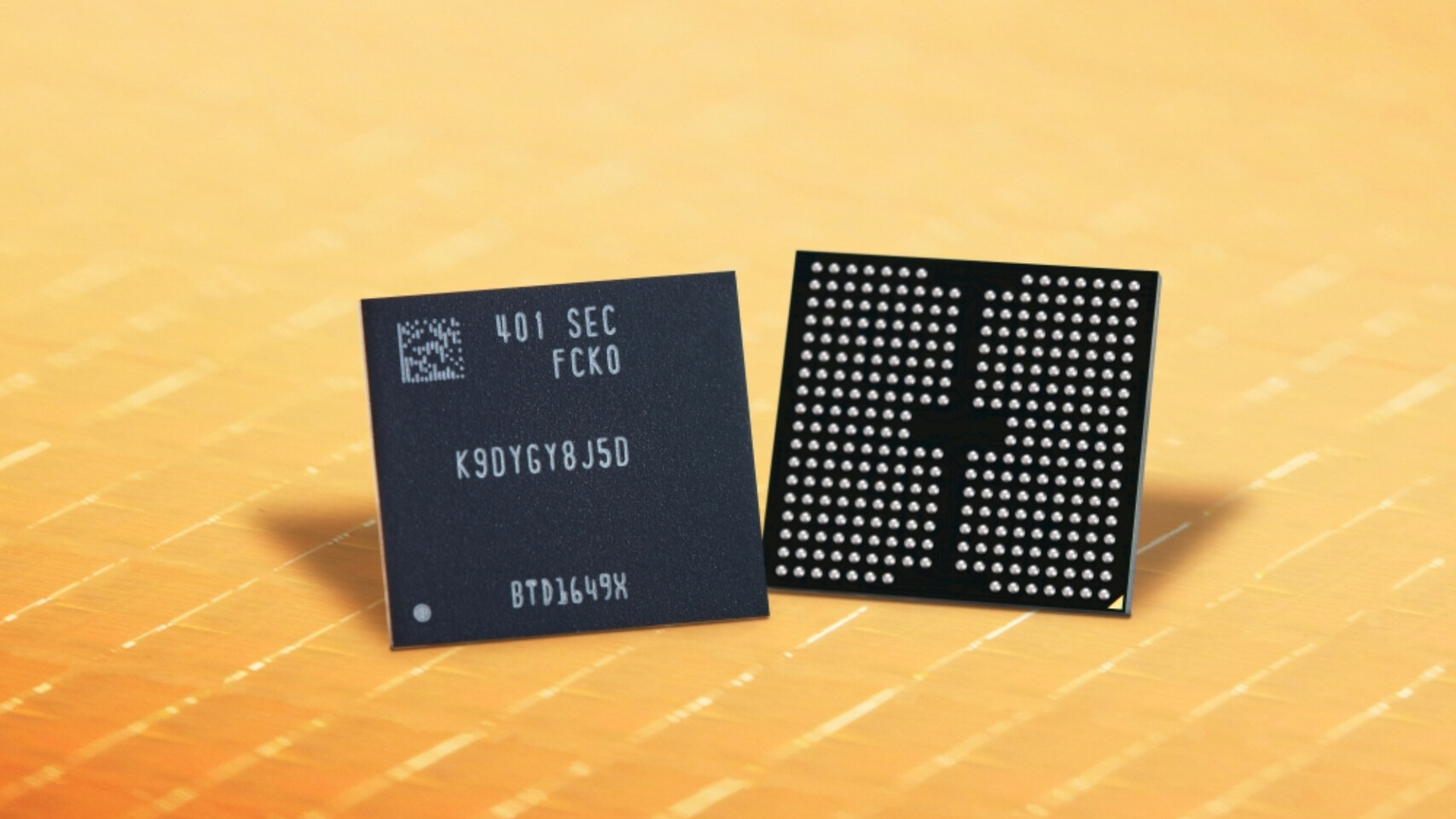
- Technology: Cell Multi-Bonding (CMB) - hybrid wafer stacking
- Layer count: 900 layers (two stacked 450-layer chips)
- Manufacturing challenge: Wafer warping and alignment corrected via proprietary chucks
- Roadmap: 10th-gen V-NAND (400+ layers) in mass production first, followed by 900-layer variant
- Competitive context: SK hynix holds current volume record at 321 layers with 4D NAND
The immediate impact is unclear for consumers. Samsung’s plan calls for ramping up its 10th-generation V-NAND (with over 400 layers per chip) before the bonded 900-layer design reaches high-volume production—likely several quarters away. While this could eventually shrink SSD form factors or boost capacity, real-world adoption hinges on manufacturing scalability and cost efficiency.
One reality check: wafer bonding at these scales isn’t trivial. Even with Samsung’s advances, overlay precision and power management remain critical hurdles. The company’s goal of 1000-layer chips by 2030 suggests this is just the first step in a longer evolution, not an overnight revolution.
For now, buyers should monitor Samsung’s production roadmap rather than storage benchmarks. If successful, this could shift the density landscape—but only after proving it works at scale.