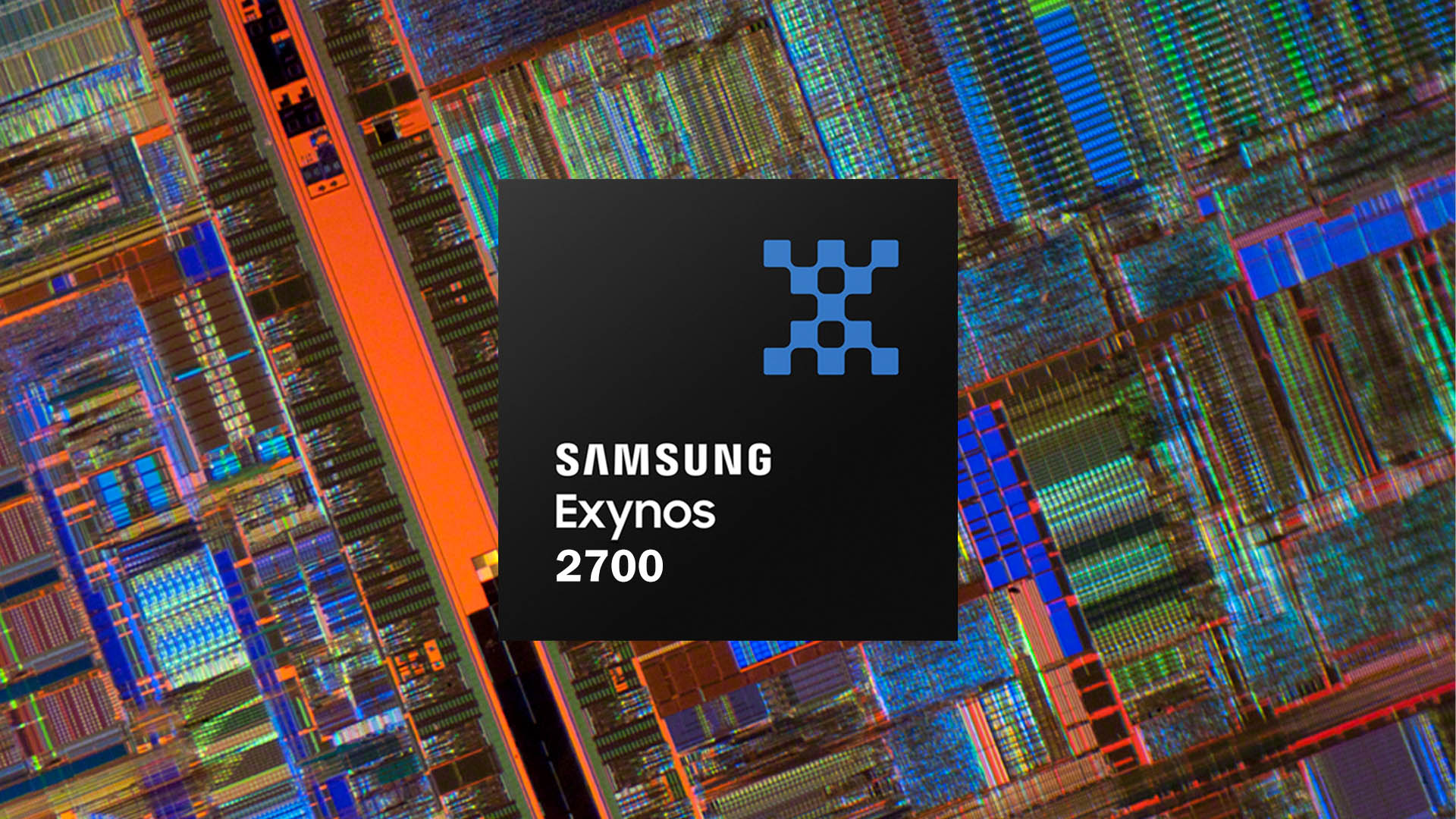
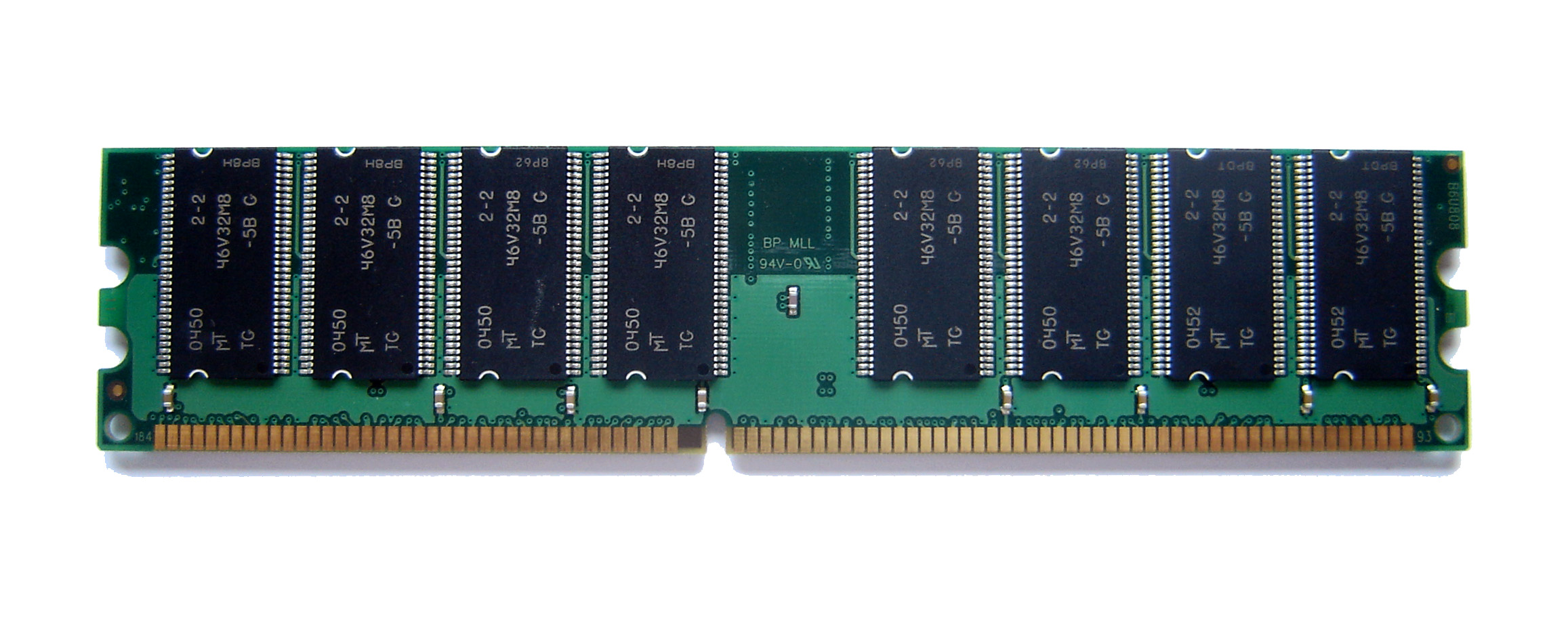
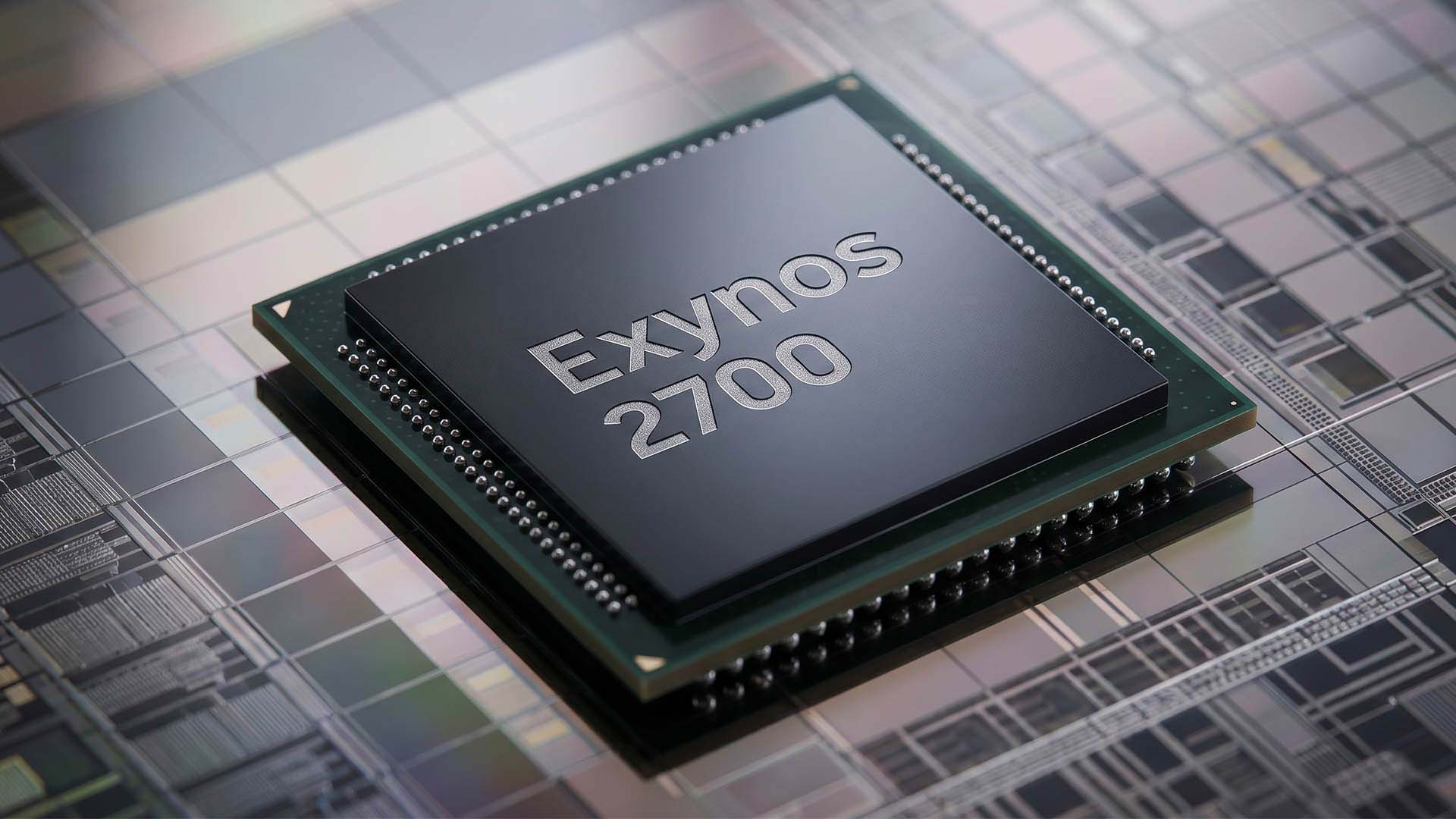
Samsung Plans To Transform Your Smartphone & Tablet Into On-Device AI Powerhouses With High-Bandwidth Memory Chips Using Complex Packaging Omar Sohail • at EDT Add on Google The latest report says that the technology will be applied to Samsung's Exynos range first How We Rate Rumors 0-20%: Unlikely - Lacks credible sources 21-40%: Questionable - Some concerns remain 41-60%: Plausible - Reasonable evidence 61-80%: Probable - Strong evidence 81-100%: Highly Likely - Multiple reliable sources RUMOR ASSESSMENT 55% Plausible High-Bandwidth Memory (HBM) won’t be limited to servers because the latest report states that Samsung is employing a unique packaging technology that will make smartphones and tablets compatible with these ultra-fast DRAM chips. The goal for the Korean giant is to turbocharge mobile devices into on-device AI beasts, and looking at the profits that Samsung is raking in during the ongoing shortage, the company surely doesn’t want to miss out on any markets. The objective is to develop HBM technology tailor-made for smartphones and tablets to prevent unnecessary space and power hurdles Traditional mobile DRAM utilizes copper wire bonding, but their I/O terminal limitations in the 128-256 range mean that there’s tremendous signal loss while boosting efficiency and lowering heat generation. According to ETNews, Samsung intends to equip smartphones and tablets with HBM using ultra-high aspect ratio copper pillars with Fan-Out Wafer Level Packaging (FOWLP), the same packaging used on SoCs like the Exynos 2600 to improve heat resistance and increase sustained workload performance. Related Story NVIDIA’s Rubin AI Platform Alone Will Devour More LPDDR Memory in 2027 Than Apple and Samsung Combined, Starving Smartphone SupplyThrough Samsung’s advancements in Vertical Copper Post Stack (VCS), the manufacturer can ensure that HBM chips thrive in mobile devices despite the size constraints by stacking DRAM dies in a “staircase” configuration and filling the gaps with copper pillars. The report states that Samsung has substantially increased the aspect ratio of copper pillars in VCS packaging from the existing 3-5:1 to 15:1–20:1, boosting bandwidth. Unfortunately, this approach will result in a reduction of the copper pillar diameter. If this diameter falls below 10 micrometers, these copper pillars can bend or worse, completely break, which is where FOWLP comes into play, offering increased structural integrity by extending the copper wiring outward. The use of FOWLP increases the number of I/O terminals as well, further contributing to a 30 percent increase in bandwidth. Since Samsung is currently developing this technology, it’s difficult to determine when mobile-based HBM will debut. Looking at the current timeline, Samsung may incorporate it in the Exynos 2800, which is reported to be the company’s first SoC to feature an in-house GPU, or the Exynos 2900. Apple is also said to bring HBM technology to its iPhones, but it’s unconfirmed if the Cupertino firm will source this technology from Samsung. Huawei is also exploring this technology, but it’s unlikely that the Korean manufacturer will enter a Chinese OEM’s supply chain. Also, given how expensive mobile DRAM has become, we believe that smartphone companies will only begin brainstorming the feasibility of HBM chips in their devices when prices stabilize. Assuming RAM remains ridiculously expensive for the next couple of years, upgrading on-device AI capabilities on smartphones and tablets may remain limited to the chipset and storage. News Source: ETNews About the : Omar Sohail is a and analyst for 's mobile section, specializing in the technology and business of the mobile industry. His expertise lies in the intricate hardware supply chain, covering developments in semiconductor manufacturing, chip lithography, and camera sensor technology. Follow on Google to get more of our news coverage in your feeds. Further Reading Chinese Memory Makers Accelerate DDR5 Development, Reaching 8000 MT/s DRAM Speeds As They Near Samsung, SK Hynix & Micron Levels Exynos 2700 To Receive Premium Treatment From Samsung As Update Drops Claims Of Company Abandoning Its 2nm SoC’s Advanced Packaging SK hynix Workers Become The Hottest Commodity In South Korea’s Marriage Mart After A $2.5 Billion Bonus Pool Hits Their Bank Accounts Samsung’s 5-Layer QD-OLED Lands First In MSI’s MAG 271QPX32, Bringing 40% Better Blacks And 320Hz At 1440p To Gamers Read all on Samsung Plans To Transform Your Smartphone & Tablet Into On-Device AI Powerhouses With High-Bandwidth Memory Chips Using Complex Packaging