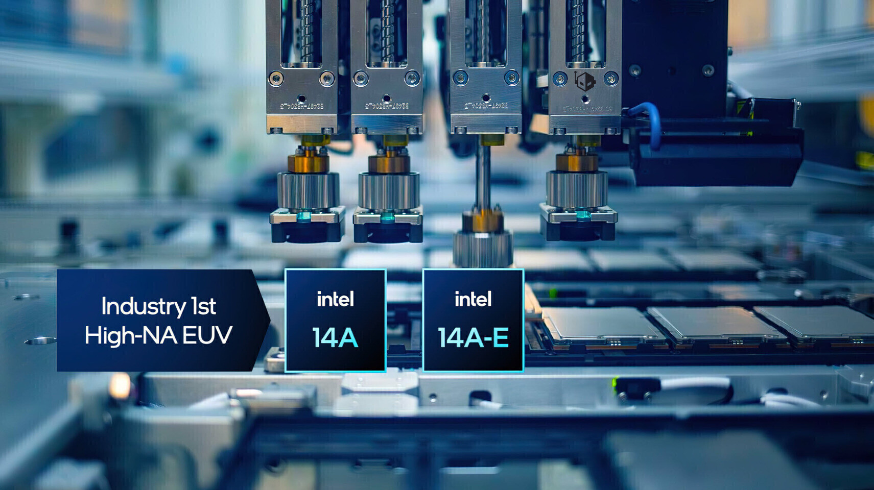
Samsung’s latest mobile processor, the Exynos 2700, has quietly emerged from the shadows of engineering labs, with benchmark data from an early test platform hinting at a major leap forward in performance and efficiency. Unlike the Exynos 2600, which will power the upcoming Galaxy S26 series using Samsung’s SF2 foundry node, the 2700 appears to be a testbed for the company’s more advanced **2 nm GAA process**, a technology Samsung has been aggressively refining to reclaim ground in the semiconductor arms race.
Leaked benchmarks from a development board labeled **S5E9975 ERD**—an acronym for Engineering Reference Design—show a **10-core CPU** paired with an **Xclipse 970 integrated GPU**, a slight upgrade from the 960 iGPU seen in earlier Exynos 2600 samples. However, the Geekbench 6.2.2 OpenCL score of **15,618** falls short of expectations, raising questions about the test environment rather than the chip’s raw capabilities.
Industry observers suggest the **ERD platform** is not a final consumer product but a validation tool designed to stress-test Android 16’s scheduling and power management systems. By mixing cores from different generations, Samsung is likely refining its **Heat Path Block (HPB)** technology—a proprietary solution to mitigate thermal throttling in high-performance mobile chips. This approach, if successful, could position the Exynos 2700 as a more stable and efficient alternative to competitors like Qualcomm’s Snapdragon 8 Gen 3.
Key Specs and What They Mean
The Exynos 2700’s benchmark data, though preliminary, paints a picture of a chip built for future-proofing

- CPU: 10-core configuration (exact architecture not confirmed, but likely a mix of high-performance and efficiency cores).
- GPU: Xclipse 970 iGPU (successor to the 960, with potential for improved ray tracing and AI acceleration).
- Process Node: **2 nm GAA (Gate-All-Around)**, Samsung’s most advanced fabrication process to date, offering better power efficiency and performance density.
- Heat Path Block (HPB): Proprietary thermal management tech to reduce heat buildup in demanding workloads.
- Test Platform: S5E9975 ERD (Engineering Reference Design), not a retail device—benchmarks are for validation, not final performance metrics.
For consumers, these specs translate to a few critical takeaways. First, the shift to **2 nm** suggests Samsung is betting heavily on its in-house foundry to compete with TSMC and Intel, particularly as demand for AI-optimized chips surges. The **HPB technology** could also address a long-standing weakness in Exynos chips—thermal throttling—making it a more viable option for flagship devices. However, the benchmark results are far from definitive; the ERD platform is likely running a mix of old and new cores for testing, which could explain the lower-than-expected scores.
While the Exynos 2700 won’t appear in consumer devices anytime soon, its development signals Samsung’s intent to push beyond the Exynos 2600’s limitations. The chip’s architecture may also influence future collaborations, with rumors already linking Samsung’s foundry to potential deals with Qualcomm and even NVIDIA for AI platforms. If the 2 nm process delivers on its promises, the Exynos 2700 could mark the beginning of a new era for Samsung’s mobile chip ambitions.
As for when this chip might reach the market, no official timeline has been confirmed. Samsung’s focus remains on ramping up production of the Exynos 2600 for the Galaxy S26 series, but the 2700’s engineering sample suggests the company is already laying the groundwork for what comes next.