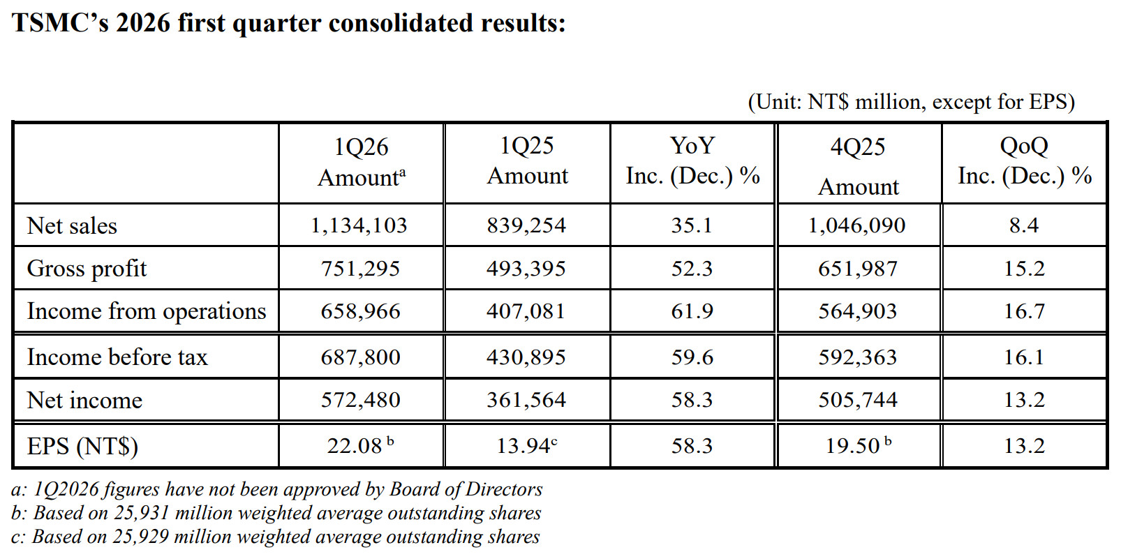
TSMC’s Q1 2026 performance paints a picture of both financial strength and strategic reinvention. Revenue climbed to NT$491 billion—a 3% increase from the previous quarter—while net income, though down 4% year-over-year, remained stable on a quarterly basis. Yet beneath these numbers lies a fundamental reorientation: advanced packaging is emerging as TSMC’s new engine of growth, one that could reshape the semiconductor ecosystem for years to come.
This shift comes at a moment of transition for the industry. TSMC still commands 65% market share in advanced nodes (3nm and below), but the rising cost of 3D stacking and packaging is forcing a reevaluation of how chips are designed, manufactured, and deployed. The question now isn’t just whether TSMC can sustain this pivot, but whether it can lead an entire industry toward a more modular, high-performance future.
A Cornerstone of the Semiconductor Ecosystem
TSMC’s strategy is deeply intertwined with the evolution of computing platforms. Its dominance in advanced nodes has long been the backbone of the semiconductor industry, but the push into advanced packaging introduces new dynamics. No longer just a foundry, TSMC is becoming a key architect of how chips are structured at the system level.
- Advanced packaging now accounts for a growing share of R&D investment, with 3D stacking and chiplet-based designs taking center stage.
- The company is targeting high-performance computing (HPC) and AI workloads as primary applications for this technology.
- Supply chain constraints, particularly in memory and substrate materials, remain a critical bottleneck, but TSMC is treating them as a catalyst rather than an obstacle.
The financial implications are already visible. Capital expenditure surged 22% year-over-year to NT$151.5 billion, reflecting the cost of this transition. While some investors may see this as a risk, TSMC views it as a necessary investment in the future—one that could pay off handsomely if it successfully positions itself at the forefront of next-generation computing architectures.
Who Stands to Gain—or Lose?
The impact of this shift will ripple through the entire semiconductor ecosystem. For enterprises, the most immediate consequence may be higher costs downstream, as advanced packaging introduces new layers of complexity and expense. However, the long-term benefits could be substantial.
- Heterogeneous designs enabled by chiplets could accelerate innovation in data centers and AI systems, offering better performance-per-watt efficiency.
- The modular nature of chiplet-based architectures may simplify procurement for enterprises, allowing them to mix and match components more flexibly.
- TSMC’s leadership in this space could set the standard for how future chips are built, influencing competitors and partners alike.
Yet challenges remain. The transition to advanced packaging is not without its hurdles: longer R&D cycles, tighter supply chain dependencies, and the risk that higher upfront costs may not translate into immediate returns. TSMC’s ability to execute on this strategy will determine whether it can maintain its unassailable position in the industry—or if it will cede ground to those who adapt more swiftly.
One thing is certain: the semiconductor platform is no longer static. TSMC’s pivot toward advanced packaging is a sign that the industry is entering a new era, one where modularity and heterogeneity are as critical as raw performance. Whether this shift sustains momentum or exposes vulnerabilities will be the defining question for TSMC—and the broader ecosystem—in the years ahead.